PRODUCTS
Optical Communication Applicat
-
Active Component Manufacturing
- Optical LD & PD Wafer
- Aspherical Lens and Cap
- TEC Device
- 2.5G-10G APD CHIP
- 10G PIN PD CHIP
- Transimpedance Amplifier
- Aluminum Nitride Substrates
- Alumina substrates
- High Temperature Co-fired Substrates (HTCC)
- 10G CWDM DFB Chip
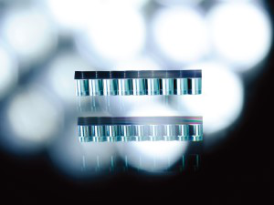
- Microlens Array
- Smile Corrector
- Slow Axis Collimators(SAC)
- Fast Axis Collimators Arrays(FACA)
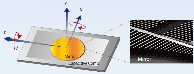
- MEMS Mirror
- SOI Wafers
- Super-thick Thermal Oxidized Wafers
- 25G DFB Laser Diode Chip
-
Test and Measurement
-
High Speed Qptical Transceiver
-
Optical Transport Network Devi
-
Network, Security and Delivery
-
Optical Automation Equipments
-
Passive Component Manufacturin
Industrial Laser and Optical A
-
Lasers
-
Laser Drivers
-
Controller Electronics
-
Optical Components
-
Materials
Solutions
-
BOSA Manufacturing and Packagi
-
ECDL Stable Laser Solution
-
Laser Spectroscopy Solution
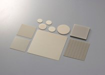
Aluminum Nitride Substrates

Features
■ High thermal conductivity (170-230W/mK), up to 9.5 times than that of Alumina
■ Similar coefficient of thermal expansion to that of silicon (Si). This helps to achieve high reliability of Si chip and thermal heat cycling
■ Higher electric insulation, and Smaller dielectric constant
■ Higher mechanical strength (450MPa).
■ Superior corrosion resistance against molten metal.
■ Very high purity, no toxicity.
Applications
Heat dissipation substrate, LED package, Power module, Wafer bonding, Power resistor.
*Various metalized processing is available (Thin film, Thick film, DBC, AMB, DPC, etc.).
Supplier

MARUWA established an integrated production system from ceramic substrates and machined substrates to electronic components or devices, so as to be responsive to the market needs. We are on a mid-way of further integrating our technical capabilities and keep on polishing our general technologies from ceramics to circuit designing and packaging.
